Gilbert Cell Mixer Design
RF Analog Circuit Design using GF180MCU Technology
Introduction and Project Overview
This project involves the design and implementation of a Gilbert cell mixer for RF applications as part of the 2025 Chipathon organized by the IEEE Solid-State Circuits Society (SSCS). The work encompasses RF circuit design, layout implementation, verification, and comprehensive performance characterization using the GF180MCU process technology.
Theory
The Gilbert cell is a type of mixer, utilizing three differential pairs. The mathematical operation of a mixer is to multiply the two input signals (RF and LO). Supposing that the two signals are sine waves with the following shape:
$$ \begin{align} & v_{RF}=A(t) \cos \left(\omega_{RF} t+\phi(t)\right) \nonumber \newline & v_{LO}=A_{LO} \cos \left(\omega_{LO} t\right) \nonumber \tag{1} \end{align} $$
the mixer will produce the following output:
$$ \begin{align} v_{\text{out}} &= v_{RF} \times v_{LO} \nonumber \newline &= \frac{A(t) A_{LO}}{2}\left[\cos \phi(t)\left(\cos \left(\omega_{LO}+\omega_{RF}\right) t+\cos \left(\omega_{LO}-\omega_{RF}\right) t\right) - \right. \nonumber \newline & \left.\quad \phantom{=\frac{A(t) A_{L}}{2}} \sin \phi(t)\left(\sin \left(\omega_{LO}+\omega_{RF}\right) t+\sin \left(\omega_{LO}-\omega_{RF}\right) t\right)\right] \nonumber \newline &= \frac{A(t) A_{LO}}{2} \left[\cos \left(\left(\omega_{LO}+\omega_{RF}\right) t+\phi(t)\right) + \right. \nonumber \newline & \left.\quad \phantom{=\frac{A(t) A_{L}}{2}} \cos \left(\left(\omega_{LO}-\omega_{RF}\right) t+\phi(t)\right)\right] \tag{2} \end{align} $$
In this derivation we have ignored the non-linearity of the mixer, thus omitting the higher order harmonics. These harmonics will become important when we discuss the linearity of the mixer.
Equation (1) demonstrates that the mixer produces two sine waves, at the frequencies $\omega_{IF}=\omega_{LO} \pm \omega_{RF}$. This property of the mixer can also be seen from a Fourier perspective, using the fact that the Fourier transform of a product of two functions is the convolution of their Fourier transforms. But we will try to keep the math to a minimum here…
A mixer is a non-linear circuit (as it includes MOSFETs, which are non-linear circuit elements), and thus its operation can be approximated by a sum of powers (ignoring higher order effects) [1]: $$ \begin{equation} y(t) \approx \alpha_1 x(t)+\alpha_2 x^2(t)+\alpha_3 x^3(t) \tag{3} \end{equation} $$ Note that this is not a Taylor expansion, but rather a fit of a part of the signal of interest.
For a sine input, $x(t)=A \cos \omega\textit{t}$, substituting into the power series from Eq.(3), we get:
$$ \begin{align} y(t) & =\alpha_1 A \sin \omega t+\alpha_2 A^2 \sin ^2 \omega t+\alpha_3 A^3 \sin ^3 \omega t \nonumber \newline & =\alpha_1 A \sin \omega t+\frac{\alpha_2 A^2}{2}(1-\cos 2 \omega t)+\frac{\alpha_3 A^3}{4}(3 \sin \omega t+\sin 3 \omega t) \nonumber \newline & =\frac{\alpha_2 A^2}{2}+\left(\alpha_1 A+\frac{3 \alpha_3 A^3}{4}\right) \sin \omega t+\frac{\alpha_2 A^2}{2} \sin 2 \omega t+\frac{\alpha_3 A^3}{4} \sin 3 \omega t \tag{4} \end{align} $$
Now, it is much clearer to see, that for a sinusioidal input, a nonlinear system will produce higher harmonic outputs.
Using a bit of imagination and the lesson we learned from the Eq.(4), it is easier to see that a mixer (being a non-linear system) will produce higher harmonics besides the fundamentals. Several mixer specifications describe how much and under what conditions these undesireable higher harmonics become important.
The Input P1dB is the input power (in dBm), at which the higher harmonics reduce the expected linear output characteristic by 1dB. Although not exact, an interpretation for the P1dB metric can be the following: what power do I need to give the input signal, in order for the higher harmonics to become ‘more significant’ in the output than the fundamentals.
References
[1] B. Razavi, RF Microelectronics, 2nd ed. Upper Saddle River, NJ: Prentice Hall, 2012, eq. 2.25.
Target specifications
The target specification of the project are given in the table below. Alongside theses specs, simlation results from ngspice are included for comparison.
| Metric | Target | Simulation | Measured |
|---|---|---|---|
| RF frequency | $89.3\text{MHz}$ | $89.3\text{MHz}$ | - |
| LO frequency | $100\text{MHz}$ | $100\text{MHz}$ | - |
| IF frequency | $10.7\text{MHz}$ | $10.7\text{MHz}$ | - |
| Conversion gain | $\geq 12\text{dB}$ | $11.55\text{dB}$ | - |
| Input P1dB | $-8\text{dBm}$ | - | - |
| IIP3 | $\leq +2\text{dBm}$ | - | - |
| Noise figure | $\leq 9\text{dB}$ | - | - |
References
[1] RF Cafe, “Mixer Characteristics and Performance,” WJ Tech Notes. [Online]. Available: https://www.rfcafe.com/references/articles/wj-tech-notes/mixers-characteristics-performance-p1.pdf
Circuit Design
In our workflow we used Xschem for creating the schematics, and a python notebook for gm/ID transistor sizing.
Gilbert cell

Transistor sizing
For the transistor sizing, we chose to use the gm/ID methodology. The RF
transistors were selected to operate in moderate inversion with gm/ID=12, since
this is the trans-conductance stage, and moderate inversion gives a good
trade-off between area, speed and gain [1-3].The switching LO transistors were
selected to operate more towards the linear triode region, but still in
moderate inversion, with a gm/Id=15. Higher gm/ID was avoided in order to avoid
having too big devices and sacrificing some of the transistor’s ft (although
the frequency response is a smaller issue, since we are working in the FM
broadcasting band). The sizing calculations were done using the pygmid python library, within a Jupyter notebook. The gm/ID calculation vs the simulation results are given in the table below:
| Source | Transistor | gm/ID | gm(mS) | ID(uA) | W(μm) | ft(GHz) | VGS(V) | VDS(V) |
|---|---|---|---|---|---|---|---|---|
| Calculation (nf=1) | RF | 12 | 0.600 | 50 | 11.64 | 7.68 | 0.69 | 1.65 |
| Calculation (nf=6) | RF | 12 | 0.600 | 50 | 10.38 | 14.34* | 0.67 | 1.65 |
| Calculation (nf=1) | LO | 15 | 0.375 | 25 | 23.84 | 2.45 | 0.64 | 1.65 |
| Calculation (nf=6) | LO | 15 | 0.375 | 25 | 20.57 | 5.28* | 0.62 | 1.65 |
| Simulation | RF | 11 | 0.55 | 50 | 10 (nf=5) | - | 0.83 | 0.39 |
| Simulation | LO | 16 | 0.42 | 25 | 20 (nf=5) | - | 0.82 | 2.23 |
Note the calculation results depend on the ’nf’ that was used in the simulations of the single device .mat files. The models which are to be used for these simulations are a bit different from the ones provided by the foundry - the correct ones are provided by B Murman on this github repo: [https://github.com/bmurmann/Chipathon2025/tree/main/models_updated_2025.07.19/ngspice].
* These fT values (14.34 GHz and 5.28 GHz) shouldn’t be trusted, since ‘cgso’ and ‘cgdo’ .op values were zero in the simulation. This means the capacitance of the G,D and S terminals are off.
References
[1] B. Boser, “OTA gm/Id Design,” UC Berkeley EECS Department, 2011-12. [Online]. Available: https://people.eecs.berkeley.edu/~boser/presentations/2011-12%20OTA%20gm%20Id.pdf
[2] “MOSFET Operation in Weak and Moderate Inversion,” StudyLib. [Online]. Available: https://studylib.net/doc/18221859/mosfet-operation-in-weak-and-moderate-inversion
[3] “Lecture Notes on Nanotransistors,” Purdue University, edX Course Materials, 2021. [Online]. Available: https://courses.edx.org/asset-v1:PurdueX+69504x+1T2021+type@asset+block@LNS_Lecture_Notes_on_Nanotransistors.final.pdf
Biasing network
The biasing network we decided to use makes use of one PMOS current mirror to produce a biasing current, which is then distributed among three identical NMOS current mirrors. This topology provides robustness in biasing parts of the chip which are physically far aprat, for which the connecting wiring can be long. By locally providing a bias current from a current mirror, this wiring length is no longer a significant contributor to mismatches.
Conected to the common gate of the tranistors in the current mirrors is a docupling capacitor, which reduces the noise in the VGS voltage.


Transistor sizing
The input current is designed to be ~10uA. The PMOS current mirror should output 30uA (since the wire carrying the PMOS mirror currend Id can be long, a rule of thumb is to use 10s of uA drive across it), equally divided across the parallel NMOS current mirrors. Current mirrors 1 and 2 should provide ~50uA of biasing to each of the branches of the Gilbert mixer; current mirror 3 should provide around 30uA bias current for the 5T-OTA; and current mirror 4 should provide around 60uA biasing to the output stage.
First, each of the current mirrors was sized with its own testbench. Below are the results using gm/Id sizing, obtained from this jupyter notebook:
| Source | Mirror | gm/ID | gm(mS) | ID(uA) | L(μm) | W(μm) | VGS(V) | VDS(V) |
|---|---|---|---|---|---|---|---|---|
| Calculation (nf=1) | PMOS | 6 | 0.06 | 10 | 0.4 | 2.15 | 1.06 | 1.65 |
| Simulation (nf=1) | PMOS | 5.6 | 0.056 | 10 | 0.4 | 2 | 1.08 | 1.08 |
| Calculation (nf=1) | NMOS | 6 | 0.06 | 10 | 1.0 | 1.5 | 0.97 | 1.65 |
| Simulation (nf=1) | NMOS | 5.7 | 0.057 | 10 | 1.0 | 1.5 | 0.99 | 0.99 |
Then, the entire biasing network was simulated, with some test resistances connected to the current bias outputs, to measure the output current.
References
[1] Analog Devices, “Chapter 14,” University Courses - Electronics. [Online]. Available: https://wiki.analog.com/university/courses/electronics/text/chapter-14
[2] Sedra and Smith, Microelectronic Circuits, International Sixth Edition, eq 7.148
Impedance matching stage

The design was then tested with a $10pF$ loading capcitor.
References
https://people.engr.tamu.edu/spalermo/ecen474/lecture11_ee474_simple_ota.pdf
![Operational Amplifier vs Operational Trans-amplifier as an impedance matching stage. Image taken from [1]](https://www.landflier.com/images/projects/gilbert_cell/Op_Amp_vs_OTA.svg)
Secondary ESD cell
A secondary ESD cell is needed to protect agains Charge Device Model (CDM). A primary ESD for Human Body Model (HBM) was included in the padframe generator, meaning it was automatically present.
The circuit of the CDM cell consists of two diodes and a resistor connected in series with the primary ESD (chip Pad), and the gate of the connected transistors.
The working of the secondary ESD is the following: suppose a large current is discharged from the the ASIG_5p pin to the to_gate port. This causes a voltage to develop across the resistor. In the case this voltage is too low or two high, the diodes will discharge this voltage to either of the power rails, and the gate of the FET won’t see that current (and voltage), thus protecting the gate. Remember, a diode operates when $V_CE > 0.7V$, and discharges ‘any’ current, regardless of what the voltage across it is (to a first approximation, given the voltage is not absurdly high/low, in which case the diode will break down).
Thus, the combination of the resistor and the two diodes connected to the power rails discharges any high voltages or currents fed to the gate of a transistor connected to the ESD CDM protection cell.

Layout Implementation
In RF and analog layout, device matching is paramount for the correct operation of the circuits. Below, we have included some tidbits and pictures on transistor layout matching:
- Dummy transistors
To ensure the same operation point for devices across the physical area of the chip, dummy structures are placed to homogenize the local environment of the devices. In [3] (which is taken from a more formal source [1]), various dummy techniques are shown for resistors, capacitors and transistors.
- Interdigited design
Current flows laterally across a CMOS (i.e from a typical Manhattan layout, right-to-left or left-to-right). These two orientations might have different mobilities, for example due to ’tilted implants’ from the ion implantation, which is done at an angle. There are other sources of orientation mismatch, such as litho misalignment (drain and source could be defined with different layers on the photo-mask level).
![Figure 13.57 from [1], example of interdigited design. This design can be labeled as dAsBdBsAD](https://www.landflier.com/images/projects/gilbert_cell/interdigited_design.png)
- Common centroid design
The main consideration when doing a common centroid design are:
COINCIDENCE: The centroids of the matched MOS transistors should coincide at least approximately. Ideally, the centroids should exactly coincide.
SYMMETRY: The array should be symmetric around both the horizontal and vertical axes.
DISPERSION: When possible, a large array should be subdivided into as many smaller arrays as possible that each satisfy the rules of coincidence and symmetry. If this can be achieved, then the larger array need not satisfy these rules; only the sub-arrays that comprise it need do so.
COMPACTNESS: The array (or each of its sub-arrays) should be as compact as possible.
ORIENTATION: Matched MOS transistors should possess equal orientations.
Some examples of common-centroid interdigited designs. Brackets denote a pattern which can be repeated a number of times, given by the superscript. Dashes denote places where S-D cannot be merged
A: $\left({ }_D A_S B_D B_S A\right)^i{ }_D$
B: $\left({ }_S A_D A\right)^i\left({ }_S B_D B\right)^j\left({ }_S A_D A\right)^i{ }_S$
C: $\left({ }_S A_D A_S B_D B_S A_D A\right)^i{ }_S$
D: $\left({ }_S A_D A_S B_D-{}_S A_D A_S-{}_D B_S A_D A\right)^i{ }_S$
E: $\left({ }_S A_D A_S B_D B_S C_D C\right)^i{ }_S\left(C_D C_S B_D B_S A_D A_S\right)^i$
- More esoteric matching (withing +-1mV and +-1& current) Refer to [2]- auto-zeroing and chopper stabilization (not used in this project).
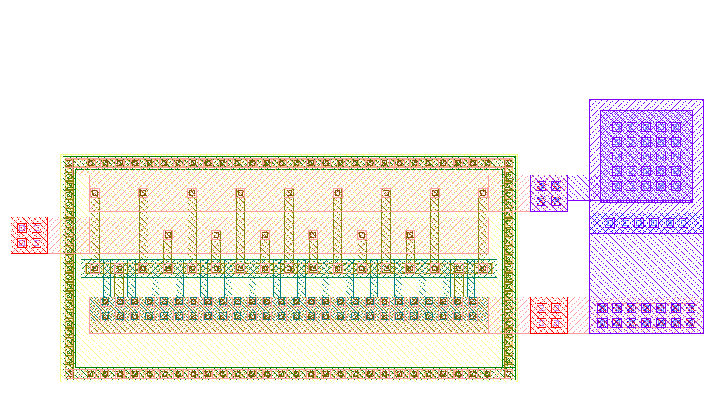
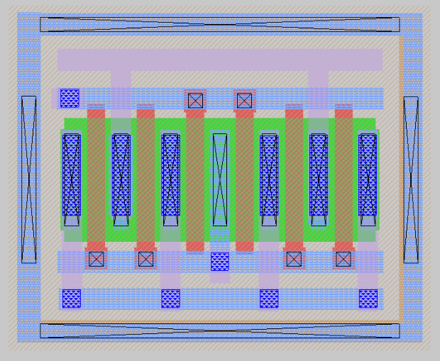
Gilbert cell
All of the layout was generated using the gLayout framework. The Gilbert mixer was generated using this python script. The layout is given below:
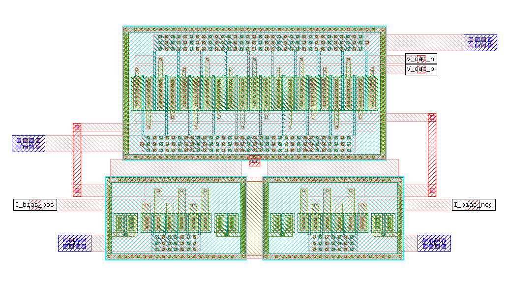
The layout was generated entirely using the gLayout framework. The two LO differential pairs are interdigited, with the $(_S A_D B_S D_D C)^i$ interdigitation scheme. Due to time constraints, the RF diff pair is generated using two ‘descrete’ gLayout NMOS FETs, each surrounded by two dummies.
References:
[1] A. Hastings, The Art of Analog Layout, 2nd ed. Upper Saddle River, NJ: Prentice Hall, 2006.
[2] C. C. Enz and G. C. Temes, “Circuit techniques for reducing the effects of op-amp imperfections: autozeroing, correlated double sampling, and chopper stabilization,” Proc. IEEE, vol. 84, no. 11, pp. 1584-1614, Nov. 1996.
[3] “Optimizing Analog Layouts: Techniques for Effective Layout Matching,” Design & Reuse. [Online]. Available: https://www.design-reuse.com/article/61548-optimizing-analog-layouts-techniques-for-effective-layout-matching/
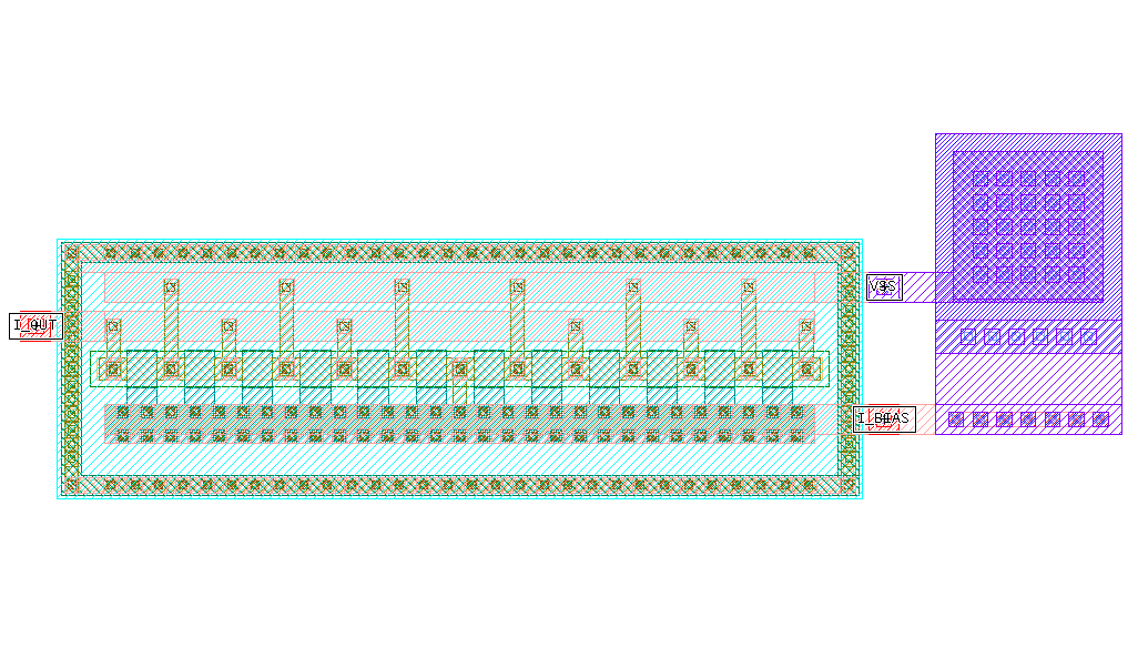
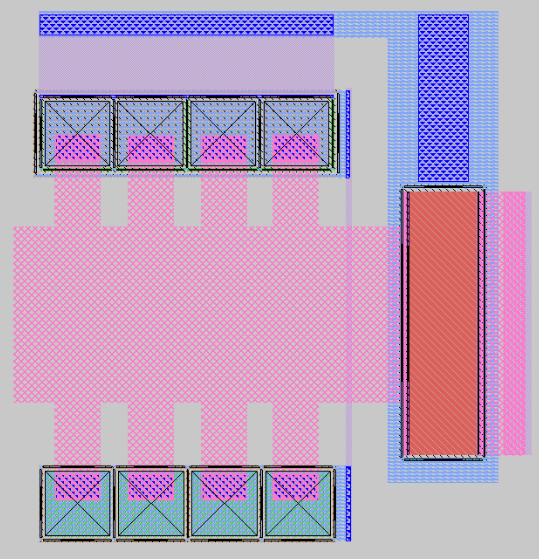
Biasing network
For the biasing network, an entirely new generator was created in the gLayout framework, which supports interdigitation of arbitrary $\frac{W}{L}$ ratios of the reference (input) FET and the mirroring (output) FET. The generator was used to create all five of the current mirrors.
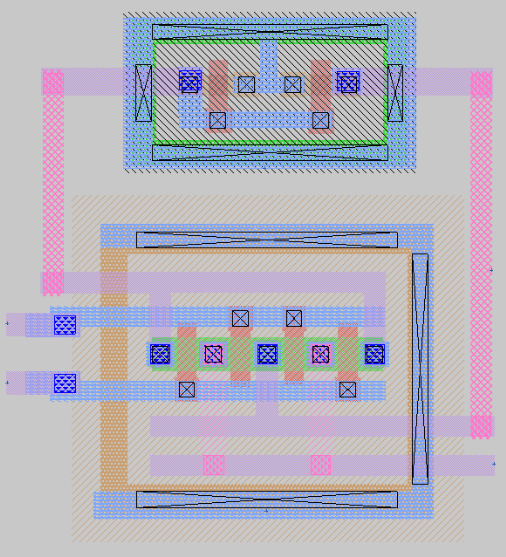
5T-OTA and CD-CD second stage
Due to time constraints, the OTA and the output stages were created by hand in Magic. Magic was very enjoyable to use, and in the future, I could work more on generators in Magic, having worked with generators in gLayout :).
Secondary protection ESD cell
According to the official GF180MCU documentation, a secondary ESD cell is necessary if the gate of a FET is directly connected to the input/output of a IO pad. The cell was laid out in Magic (and was used by other teams, which was awesome).
Verification & Analysis
Gilbert cell
Below are given waveforms for the output of the Gilbert mixer, in both the time and frequency domain. The circuit biasing is with ideal current sources, and both the RF and LO signals each contain a single frequency


Biasing network
Simulating the output of the biasing network was straighforward, using a 1ns transient simulation in ngspice. The output currents are annoted using a ammeter xschem symbol. The resistors are present in order to measure the output current across some load.

Secondary ESD protection
Below are the results of simulating the secondary CDM ESD cell’s DC and AC (in series with the primary ESD).


For the AC simulation, a $1 k\Omega$ resistor is connected at the input of the PAD port. A test AC voltage source is connected to the other port of the resistor.


Top level


Testing results
The following testing equipment will be used to measure the mixer performance:
- Vector Network Analyzer (VNA) : Measures insertion loss, return loss, and isolation.
- Spectrum Analyzer : Analyzes frequency response and spurious signals.
- Signal Generators : Provides RF, LO, and IF signals for testing.
- Power Meter : Measures power levels at different ports.
- Noise Figure Analyzer : Evaluates noise characteristics of the mixer.
The test setups for the different measurements are schematically shown in the figures below.
![Conversion loss measurement setup. DBM stands for Double Balanced Mixer, the terminations are $10dB=50Ohm$. Figure from [3]](https://www.landflier.com/images/projects/gilbert_cell/Application_Note_AN009-Mini-Circuits-004.svg)
![Two-tone third order distortion (IIP3). Figure from [3]](https://www.landflier.com/images/projects/gilbert_cell/Application_Note_AN009-Mini-Circuits-003.svg)
![VSWR measurement setup. Figure from [3].](https://www.landflier.com/images/projects/gilbert_cell/Application_Note_AN009-Mini-Circuits-002.svg)
![Isolation measurement setup. Figure from [3].](https://www.landflier.com/images/projects/gilbert_cell/Application_Note_AN009-Mini-Circuits-001.svg)
For our chip, we used the following pin-out:

References
[1] Test & Measurement World, “RF Mixer Testing.” [Online]. Available: https://www.test-and-measurement-world.com/measurements/rf/rf-mixer-testing
[2] Mini-Circuits, “Application Notes.” [Online]. Available: https://www.minicircuits.com/applications/application_notes.html
[3] Mini-Circuits, “Application Note AN00-009.” [Online]. Available: https://www.minicircuits.com/appdoc/AN00-009.html
Further tools reference websites:
[1] H. Pretl, “Magic VLSI Keybind Cheatsheet,” IIC-OSIC. [Online]. Available: https://raw.githubusercontent.com/hpretl/iic-osic/main/magic-cheatsheet/magic_cheatsheet.pdf
Notes about tool specificities, caveats
The open-source design tools are constantly evolving, and thus there were some aha’s and caveats I encountered during the design. I have listed these here to remind myself in the future.
- For a MOSFET device in the PDK, ’nf’ in MagicVLSI and ’nf’ in Xschem are completely different. Example: a device with W=2um, nf=2 in Magic will have width=W*nf=4um; the same device will have width=W=2um in xschem, with per-finger length of W/nf=1um. Steffan Schippers (the maintainer of Xschem), has even included devices which specify W as the per-finger width: Open Source Silicon Community, “In Xschem, when using such a symbol, the nf one and then havin,” Forum Discussion. [Online]. Available: https://web.open-source-silicon.dev/t/16920148/in-xschem-when-using-such-a-symbol-the-nf-one-and-then-havin. After a short discussion on the FOSSi Element chat, Tim Edwards has changed the Magic-VLSI generators to conform to the BSIM4 convention, that W is the total width, nf is the number of fingers, and thus each finger has a length W/nf. I have also pushed a pull request to the gLayout github repository to conform to this convention too, since the generators in gLayout were not adhering to it.
Some circuit design notes
Gilbert mixer
- Problem
Although the circuit is working, I am still having trouble understanding the regions of operation of the MOSFETs. For the LO devices, they should be operating as switches, however they are also hogging the entire voltage headroom. I.e VDS
2.5V for the LOs, and for the RF devices, VDS0.1-0.3 (depending on what part of the LO cycling the transistor is in). Thus, aren’t the RF FETs operating in the triode region? For both the LO and RF transistors, VGS>Vth, but for the LO VDS>VGS-Vth (i.e transistor is in saturation), but for the RF, VDS is less than VGS-Vth (i.e linear, triode region). - Solution: Could it that the the transistors are not biased correctly? To reproduce the problem the waveforms used are V_CM_rf = 1.2V, V_amp_rf=0.2V, V_CM_lo=1.2V, V_amp_lo=0.2V. Try increasing V_CM_lo, to bias the LO transistors further into saturation, forcing the VDS_lo drop to be higher across the LO transistors (so that the load network formed by the two resistors does not hog all the voltage)
Chipathon 2025 Initiative
This project is part of the IEEE SSCS Chipathon 2025, an initiative to promote hands-on IC design experience and foster innovation in the solid-state circuits community. The Chipathon provides:
- Access to industry-standard PDKs and tools
- Fabrication opportunities for student designs
- Mentorship from industry experts
- Platform for sharing design methodologies
Acknowledgments
Grateful acknowledgment to the IEEE Solid-State Circuits Society for organizing the Chipathon initiative, GlobalFoundries for providing the GF180MCU PDK access, and the broader IC design community and FOSSi organization for their support and collaboration.
Tools and Technologies
- Magic VLSI: Open-source VLSI layout editor with advanced DRC/LVS capabilities. Documentation
- GLayout: Python-based parametric layout generator for analog circuits. Documentation
- CACE: Circuit Automatic Characterization Engine for analog and mixed-signal circuit characterization. Documentation
- Xschem and Ngspice: Open-source schematic capture and SPICE circuit simulator for analog design verification. Xschem Documentation
- GF180MCU PDK: GlobalFoundries 180nm process design kit
- Python: Custom analysis scripts and data processing
Additional Resources
Educational Video
Video explaining and testing a descretely implemented Gilbert mixer.
History and reasons behind implementing a mixer in RF systems.
A very nice instructionon the measurement of IIP3 near the end of the video